

A three-terminal semiconductor device that uses both electrons and holes as charge carriers. It is mainly used for amplification and switching applications.
It consists of three terminals:
- Emitter (E)
- Base (B)
- Collector (C)
It has two P-N junctions:
- Emitter-Base Junction (EBJ)
- Collector-Base Junction (CBJ)
A small base current controls a much larger collector current, which is the fundamental operating principle of the transistor.
Types of BJT
Based on the arrangement of semiconductor materials, BJTs are classified into two types.
1. NPN Transistor
The emitter and collector are N-type, and the base is P-type.
- Majority carriers are electrons
- Most commonly used transistor
- Faster operation compared to PNP
2. PNP Transistor
The emitter and collector are P-type, and the base is N-type.
- Majority carriers are holes
- Operates with opposite polarity voltages compared to NPN
Structure of a BJT
Consists of three differently doped regions arranged in a single semiconductor crystal. The doping level of each region determines its function.
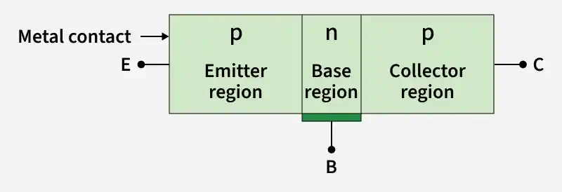
Emitter
Responsible for supplying charge carriers to the base region.
- The emitter-base junction is forward biased during normal operation.
- Responsible for supplying charge carriers to the base region.
- Heavily doped to ensure a large number of majority carriers are available.
- Due to heavy doping, the emitter has high injection efficiency.
Base
Lies between the emitter and collector and plays a controlling role in transistor action.
- A small base current controls a much larger collector current.
- Very thin compared to the other two regions.
- Lightly doped, which reduces recombination of charge carriers.
- Because of its thin width, most of the injected carriers from the emitter can cross into the collector.
Collector
Collects the charge carriers that successfully cross the base region.
- The collector-base junction is reverse biased in active mode.
- Moderately doped, less than the emitter but more than the base.
- Physically larger in size to dissipate heat generated during operation.
- Designed to handle higher reverse voltage without breakdown.
Currents in a BJT (Active Mode)
Most important mode of operation because the transistor functions as an amplifier in this region. In active mode, proper biasing allows charge carriers injected from the emitter to reach the collector, resulting in controlled current amplification.
In active operation:
- Emitter-Base Junction : Forward biased
- Collector-Base Junction : Reverse biased
Forward bias at the emitter junction enables carrier injection, while reverse bias at the collector junction ensures that the majority of these carriers are swept into the collector.
For a PNP transistor :
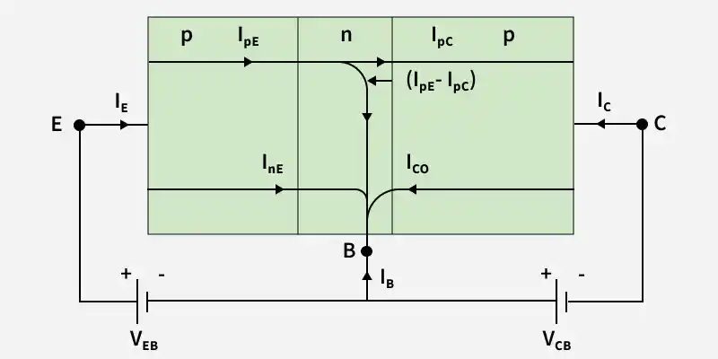
Current Components in BJT
Different current components flow inside the transistor due to charge carrier movement.
Let:
I_E = Emitter currentI_B = Base currentI_C = Collector currentI_{pE} = Hole current from emitter to baseI_{nE} = Electron current from base to emitterI_{pC} = Hole current reaching collectorI_{CO} = Reverse saturation current
Emitter Current
Sum of hole and electron currents.
I_E = I_{pE} + I_{nE} - As emitter is heavily doped :
I_{pE} >> I_{nE} - Thus, emitter current mainly consists of majority carriers.
Collector Current
Some carriers recombine in the base, and the remaining reach the collector.
- If emitter is open :
I_C = I_{CO} - In active mode :
I_C = \alpha I_E + I_{CO}
Parameters
Describe how efficiently the transistor transfers current from input to output. These parameters are important for circuit analysis and design.
1. Emitter Injection Efficiency (\gamma )
Represents how effectively the emitter injects majority carriers into the base.
For PNP transistor :
Higher
2. Base Transport Factor (\beta^{*} )
Indicates the fraction of injected carriers that reach the collector.
A higher value means less recombination in the base region.
3. Large Signal Current Gain (\alpha )
The current gain in common-base configuration. It relates collector current to emitter current.
Other relations :
Typical range :
4. Common Emitter Current Gain (\beta )
Most important and commonly used transistor parameter. It represents the ratio of collector current to base current.
Important relations :
I_B = \frac{I_C}{\beta} I_E = \frac{\beta + 1}{\beta} I_C \alpha = \frac{\beta}{\beta + 1} \beta = \frac{\alpha}{1 - \alpha}
Typical values of
5. Collector-Base Reverse Current (I_{CBO}
)
Reverse leakage current flowing from collector to base when emitter is open.
- Very small (nanoampere range)
- Depends on reverse voltage
- Doubles approximately for every 10°C rise in temperature
6. Collector-Emitter Leakage Current (I_{CEO} )
When the base is open, the collector current is called collector-emitter leakage current.
It is larger than
Regions of Operation
The BJT can operate in four different regions depending on the biasing of its junctions. The region of operation determines whether the transistor works as a switch or an amplifier.
| Region | B-E Junction | B-C Junction | Application |
|---|---|---|---|
| Cut-off | Reverse | Reverse | OFF switch |
| Active | Forward | Reverse | Amplifier |
| Saturation | Forward | Forward | ON switch |
| Reverse Active | Reverse | Forward | Rarely used |
Determining Region of Operation in Circuit Problems
In numerical problems, the region of operation of a BJT is not directly given. It must be determined by assuming a region and verifying whether the circuit conditions satisfy that assumption.
Follow these steps:
1. In switching circuits assume saturation; in amplifier circuits assume active region.
2. Use standard voltage values:
For Silicon:
V_{BE} \approx 0.7 - 0.8\,V V_{CE(\text{sat})} \approx 0.2\,V
For Germanium:
V_{BE} \approx 0.2 - 0.3\,V V_{CE(\text{sat})} \approx 0.1\,V
3. Solve the circuit equations.
4. Verify whether calculated currents and voltages satisfy the saturation condition.
If the assumptions are not satisfied, the transistor operates in another region (usually active).
Applications of BJT
Widely used in electronic circuits due to its ability to amplify signals and operate as a switch. Some major applications include:
- Signal Amplifiers : Used in audio amplifiers, radio frequency amplifiers, and small-signal amplification circuits.
- Electronic Switching : Operates in cut-off and saturation regions to function as an ON/OFF switch in digital circuits.
- Oscillator Circuits : Used in feedback-based oscillator circuits to generate periodic signals.
- Current Mirrors and Active Loads : Used in analog integrated circuits for constant current generation.
- Voltage Regulation Circuits : Helps maintain stable output voltage in power supply systems.
