

A p–n junction diode is a two-terminal semiconductor device made by joining a p-type semiconductor and an n-type semiconductor. It allows electric current to flow mainly in one direction and blocks it in the opposite direction.
Formation of P-N Junction
A p–n junction is formed by doping different regions of the same semiconductor crystal to create p-type and n-type regions.
For example, consider a thin p-type silicon sheet. By adding a small amount of a pentavalent impurity to a portion of it, that region becomes n-type, forming a p–n junction. After its formation, diffusion and drift occur. Holes diffuse from the p-side to the n-side, while electrons diffuse from the n-side to the p-side, producing a diffusion current.
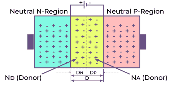
As electrons diffuse from the n-side to the p-side, they leave behind positively charged donor ions on the n-side. Similarly, holes diffusing from the p-side to the n-side leave behind negatively charged acceptor ions on the p-side. This forms the depletion region near the junction. The resulting electric field, directed from the positive n-side toward the negative p-side, causes charge carriers to move by drift. The drift current flows in the direction opposite to the diffusion current.
Biasing Conditions for p-n Junction Diode
In a p-n junction diode, there are two operational regions:
- p-type
- n-type
The voltage applied determines one of three biasing conditions for p-n junction diodes:
- There is no external voltage provided to the p-n junction diode while it is at zero bias.
- Forward bias: The p-type is linked to the positive terminal of the voltage potential, while the n-type is connected to the negative terminal.
- Reverse bias: The p-type is linked to the negative terminal of the voltage potential, while the n-type is connected to the positive terminal.
Forward Biased PN Junction
The p-n junction is said to be forward-biased when the p-type is connected to the positive terminal of the battery and the n-type to the negative terminal. The built-in electric field at the p-n junction and the applied electric field are in opposing directions when the p-n junction is forward biased.
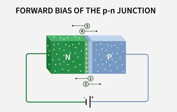
Where:
- 1- Electric field due to the battery
- 2- Built-in electric field
- 3- Direction of coventional current
- 4- Direction of electron current
The resulting electric field is smaller than the built-in electric field when both electric fields are added together. As a result, the depletion area becomes less resistant and thinner. When the applied voltage is high, the resistance of the depletion zone becomes insignificant. At 0.6 V, the resistance of the depletion area in silicon becomes absolutely insignificant, allowing current to flow freely over it.
Reverse Biased PN Junction
The p-n junction is said to be reverse-biased when the p-type is linked to the negative terminal of the battery and the n-type is attached to the positive side. The applied electric field and the built-in electric field are both in the same direction in this situation.
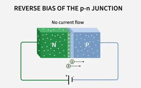
Where:
- 1- Battery induced electric field
- 2- Built-in electric field
The resultant electric field is in the same direction as the built-in electric field, resulting in a more resistive, thicker depletion zone. If the applied voltage is increased, the depletion area becomes more resistant and thicker.
P-N Junction Formula
The p-n junction formula, which is based on the built-in potential difference generated by the electric field, is as follows:
\bold{E_o = V_T\ln \left[ \dfrac{N_D - N_A}{n_i^2} \right]} where,
- The zero-bias junction voltage is E0.
- At room temperature, VT is the thermal voltage of 26 mV.
- The impurity concentrations are denoted by the letters ND and NA.
- The intrinsic concentration is denoted by ni
Current Flow in PN Junction Diode
When the voltage is increased, electrons move from the n-side to the p-side of the junction. The migration of holes from the p-side to the n-side of the junction occurs in a similar manner as the voltage rises. As a result, a concentration gradient exists between the terminals on both sides.
There will be a movement of charge carriers from higher concentration regions to lower concentration regions as a result of the development of the concentration gradient. The current flow in the circuit is caused by the movement of charge carriers inside the p-n junction.
VI Characteristics of PN Junction Diode
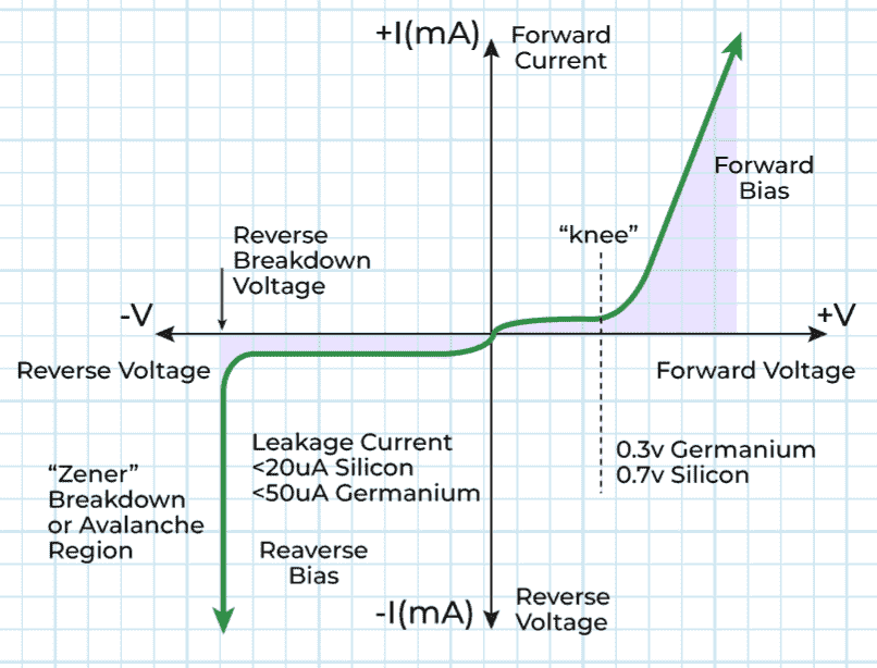
A curve between the voltage and current across the circuit defines the V-I properties of p-n junction diodes. The x-axis represents voltage, while the y-axis represents current. The graph above shows the V-I characteristics curve of the p-n junction diode. With the help of the curve, we can see that the diode works in three different areas, which are:
- Zero bias
- Forward bias
- Reverse bias
Zero Bias
There is no external voltage provided to the p-n junction diode while it is at zero bias, which implies the potential barrier at the junction prevents current passage.
Forward bias
When the p-n junction diode is in forwarding bias, the p-type is linked to the positive terminal of the external voltage, while the n-type is connected to the negative terminal. The potential barrier is reduced when the diode is placed in this fashion. When the voltage is 0.7 V for silicon diodes and 0.3 V for germanium diodes, the potential barriers fall, and current flows.
The current grows slowly while the diode is under forwarding bias, and the curve formed is non-linear as the voltage supplied to the diode overcomes the potential barrier. Once the diode has crossed the potential barrier, it functions normally, and the curve rises quickly as the external voltage rises, yielding a linear curve.
Reverse Bias
When the PN junction diode is under negative bias, the p-type is linked to the negative terminal of the external voltage, while the n-type is connected to the positive terminal. As a result, the potential barrier becomes higher. Because minority carriers are present at the junction, a reverse saturation current occurs at first.
When the applied voltage is raised, the kinetic energy of the minority charges increases, affecting the majority charges. This is the point at which the diode fails. The diode may be destroyed as a result of this.
Applications of PN Junction Diode
There are various applications of PN junction diodes in the field of electronics; some of those applications are listed as follows:
- A most common use case of a PN junction diode is as a rectifier, which means converting AC current into DC current.
- A Zener diode (which is a special type of PN junction diode) is used in circuits for voltage regulation.
- As a diode only conducts current in forward bias, in electrical circuits, it is used as a switch to turn on and off certain small circuits in a much more complex circuit.
- A reverse-biased p-n junction diode is utilized as a photodiode, as it is sensitive to light.
- An LED is also a special type of PN junction diode on a forward basis that emits light.
